

On the semiconductor line, wafer dicing leaves behind UV-tape residue that has to lift clean—and fast. If the debonding step hesitates, you’re risking micro-scratches, yield loss, and a bottleneck that ties up the whole front-end. The real question isn’t just raw power; it’s controlling the spectrum.
What matters, technically
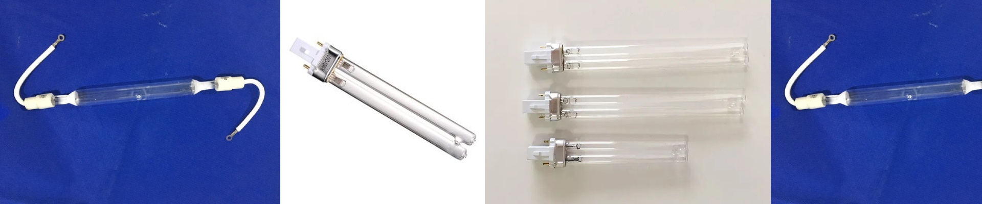
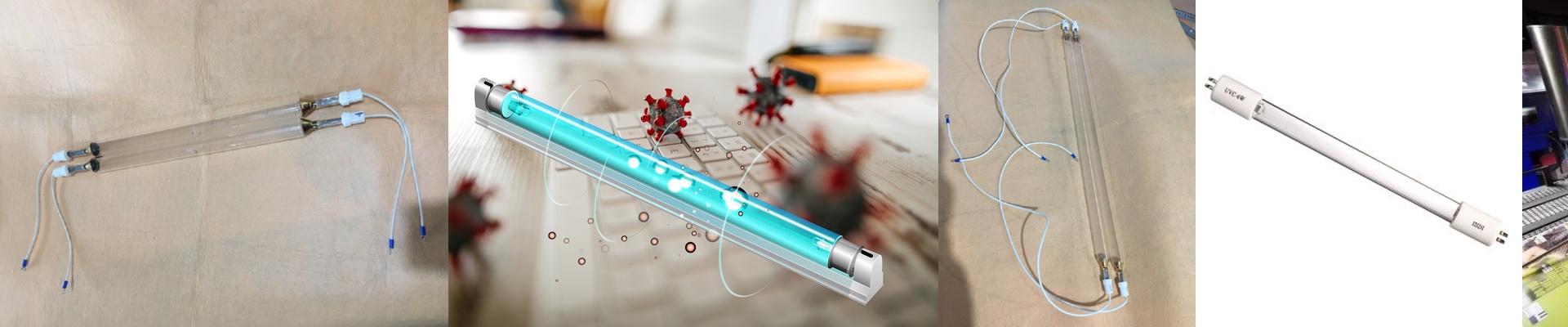
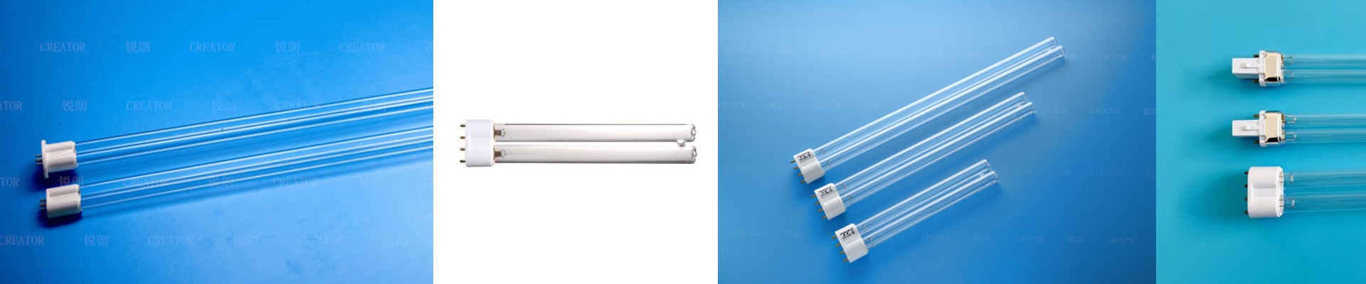
UV debonding is a photochemical trigger, not a heat soak. You need the lamp output to line up with the tape’s photoinitiator absorption—most of these UV-sensitive adhesives peak around 365 nm. We hit that peak with a high-pressure mercury vapor lamp and a dichroic-coated reflector, so the spectral output stays stable and the irradiance is consistent across the target.
We specify output as peak irradiance (mW/cm²) at a defined working distance, and the total delivered energy as dose (mJ/cm²). With the right optics, you get rapid breakdown of the cross-linking and a clean release, without overheating the adjacent films.
Why it works in wafer processing
Speed is worthless if you lose control. The lamp system is tuned so the energy density hits the tape’s activation threshold quickly—then it stops. The payoff is a predictable debonding window: minimal dwell, low thermal load, and a clean lift that keeps diced die intact.
That means shorter cycle times, fewer rejects from edge damage, and steady throughput. Energy use drops too, because the dwell is short and the optical efficiency is high—less scatter, more useful photons actually reaching the tape.
Here are the practical details
Installation has to lock in strict alignment to the bond line and a repeatable working distance. Irradiance follows the inverse square, so small shifts in position change the dose. Check your chamber geometry and any shielding—some windows will attenuate specific wavelengths.
And plan for lamp replacement around the end-of-life curve. Output decay is gradual, but it’s measurable, so schedule recalibration to keep dose repeatability where it needs to be।